-
Crosstalk-mitigated microelectronic control for optically-active spins
Hao-Cheng Weng, John G. Rarity, Krishna C. Balram, Joe A. Smith
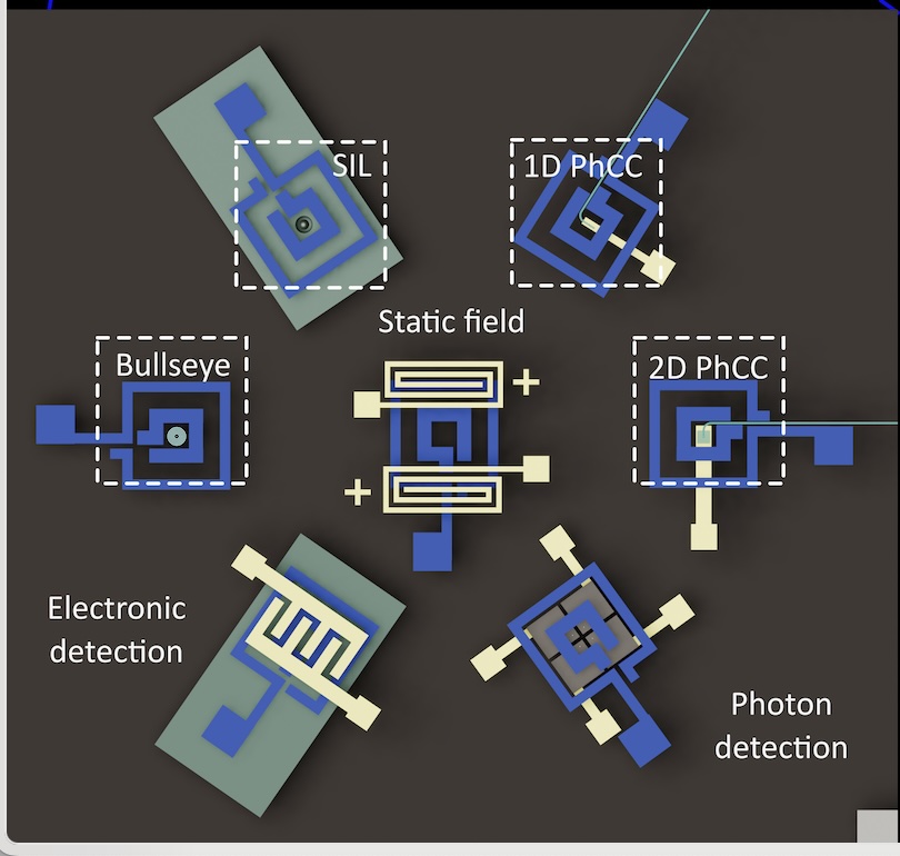
arXiv:2404.04075To exploit the sub-nanometre dimensions of qubits for large-scale quantum information processing, corresponding control architectures require both energy and space efficiency, with the on-chip footprint of unit-cell electronics ideally micron-scale. However, the spin coherence of qubits in close packing is severely deteriorated by microwave crosstalk from neighbouring control sites. Here, we present a crosstalk-mitigation scheme using foundry microelectronics, to address solid-state spins at sub-100 um spacing without the need for qubit-detuning. Using nitrogen-vacancy centres in nanodiamonds as qubit prototypes, we first demonstrate 10 MHz Rabi oscillation at milliwatts of microwave power. Implementing the active cancellation, we then prove that the crosstalk field from neighbouring lattice sites can be reduced to undetectable levels. We finally extend the scheme to show increased qubit control, tripling the spin coherence under crosstalk mitigation. Compatible with integrated optics, our results present a step towards scalable control across quantum platforms using silicon microelectronics.
Arxiv link at https://arxiv.org/abs/2404.04075 -
Robotic vectorial field alignment for spin-based quantum sensors
Joe A Smith, Dandan Zhang, Krishna C. Balram
Advanced Science 11.2 (2024): 2304449Developing practical quantum technologies will require the exquisite manipulation of fragile systems in a robust and repeatable way. As quantum technologies move towards real world applications, from biological sensing to communication in space, increasing experimental complexity introduces constraints that can be alleviated by the introduction of new technologies. Robotics has shown tremendous technological progress by realising increasingly smart, autonomous and highly dexterous machines. Here, we show that a robot can sensitise an NV centre quantum magnetometer. We demonstrate that a robotic arm equipped with a magnet can traverse a highly complex experimental setting to provide a vector magnetic field with up to 1∘ angular accuracy and below 0.1 mT amplitude error, and determine the orientation of a single stochastically-aligned spin-based sensor. Our work opens up the prospect of integrating robotics across many quantum degrees of freedom in constrained environments, allowing for increased prototyping speed, control, and robustness in quantum technology applications.
See the University of Bristol press release
Arxiv link at https://arxiv.org/abs/2305.17027 -
Heterogeneous integration of solid state quantum systems with a foundry photonics platform
Hao-Cheng Weng, Jorge Monroy-Ruz, Jonathan C. F. Matthews, John G. Rarity, Krishna C. Balram, Joe A Smith
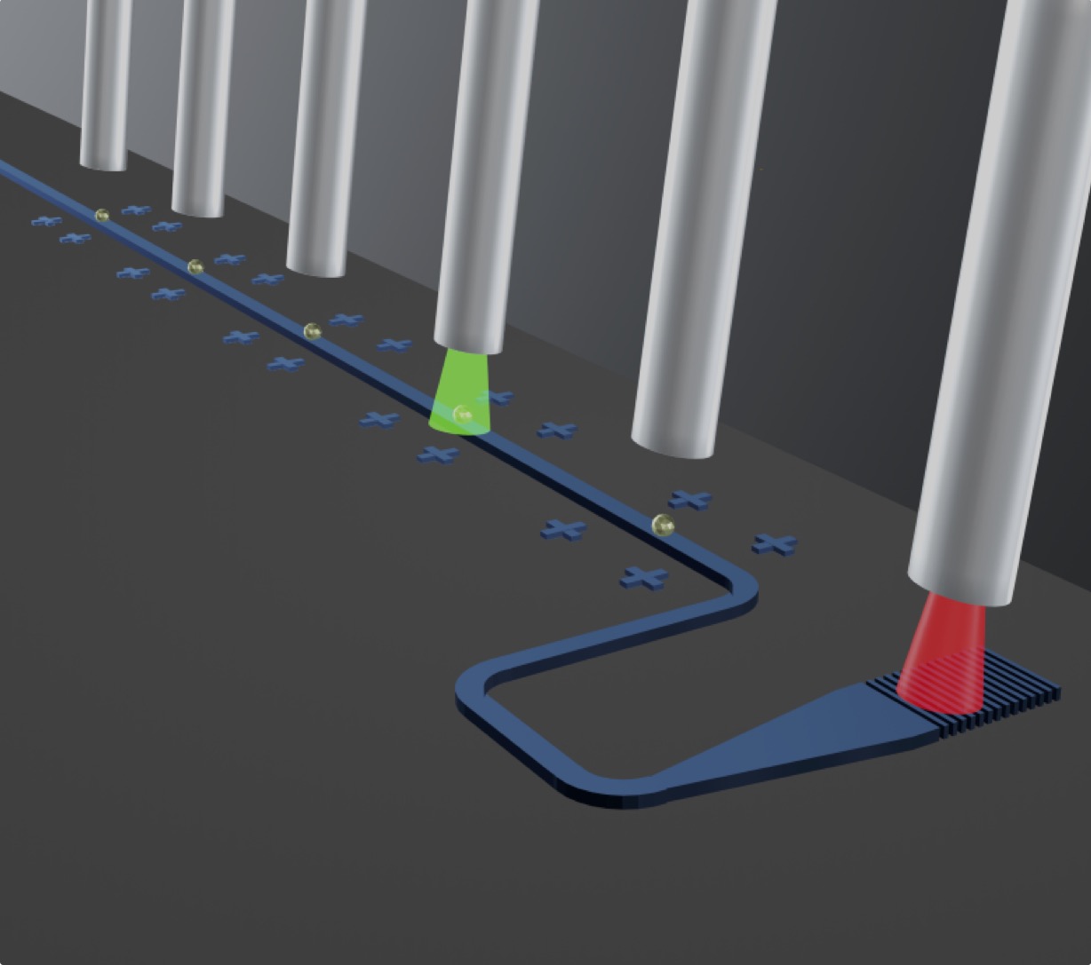
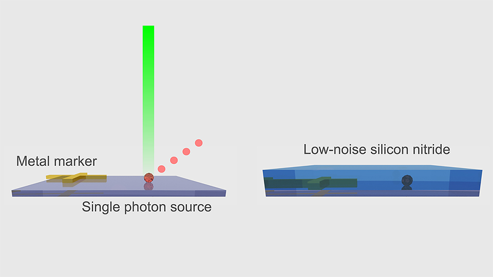
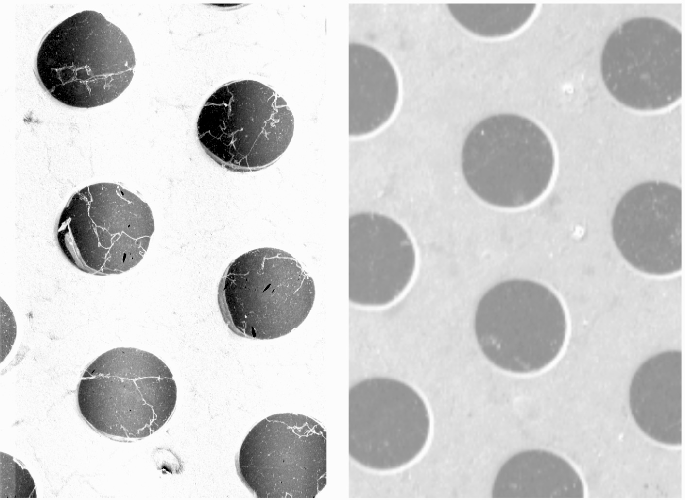
ACS Photonics 10.9 (2023):3302–3309Diamond colour centres are promising optically-addressable solid state spins that can be matter-qubits, mediate deterministic interaction between photons and act as single photon emitters. Useful quantum computers will comprise millions of logical qubits. To become useful in constructing quantum computers, spin-photon interfaces must therefore become scalable and be compatible with mass-manufacturable photonics and electronics. Here we demonstrate heterogeneous integration of NV centres in nanodiamond with low-fluorescence silicon nitride photonics from a standard 180 nm CMOS foundry process. Nanodiamonds are positioned over pre-defined sites in a regular array on a waveguide, in a single post-processing step. Using an array of optical fibres, we excite NV centres selectively from an array of six integrated nanodiamond sites, and collect the photoluminescence (PL) in each case into waveguide circuitry on-chip. We verify single photon emission by an on-chip Hanbury Brown and Twiss cross-correlation measurement, which is a key characterisation experiment otherwise typically performed routinely with discrete optics. Our work opens up a simple and effective route to simultaneously address large arrays of individual optically-active spins at scale, without requiring discrete bulk optical setups. This is enabled by the heterogeneous integration of NV centre nanodiamonds with CMOS photonics.
Arxiv link at https://arxiv.org/abs/2304.1022 -
Towards compact high-efficiency grating couplers for visible wavelength photonics
Joe A Smith, Jorge Monroy-Ruz, Pisu Jiang, John G. Rarity, Krishna C. Balram
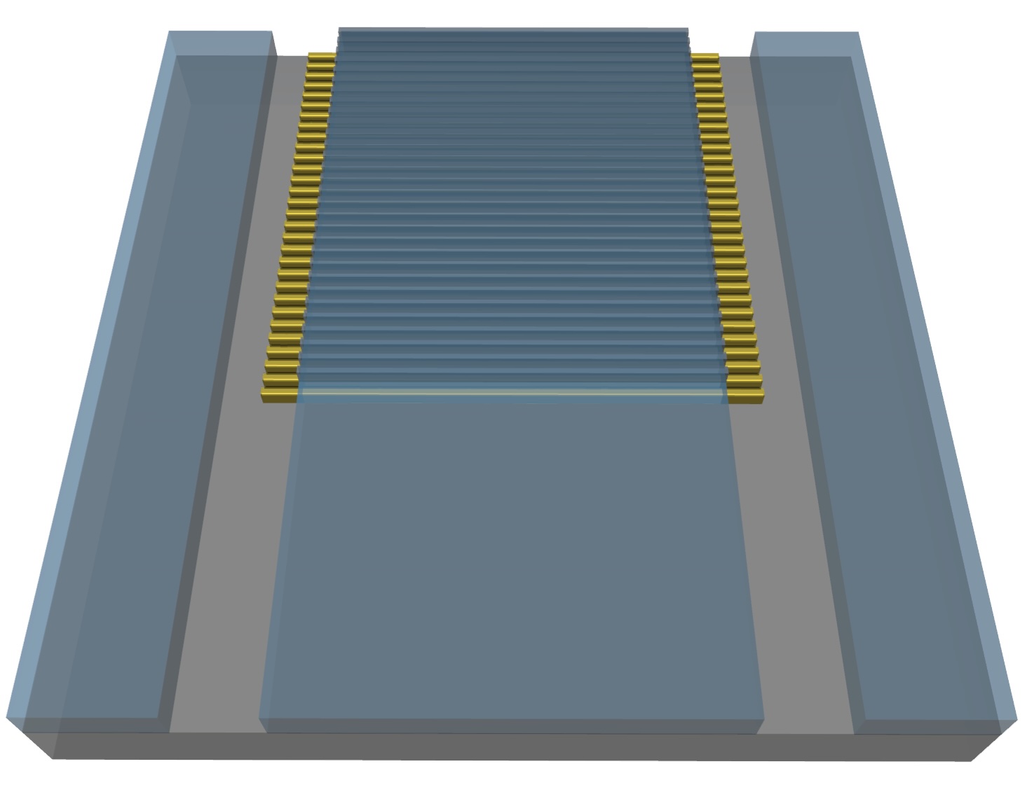
Optics Letters 47.15 (2022): 3868-3871.Although grating couplers have become the de-facto standard for optical access to integrated silicon photonics platforms, their performance at visible wavelengths, in moderate index contrast platforms such as silicon nitride, leaves significant room for improvement. In particular, the index contrast governs the diffraction efficiency per grating tooth and the resulting overall coupler length. In this work, we develop two approaches to address this problem: a dielectric grating that sums multiple optical modes to increase the overall output intensity; and an embedded metal grating that enhances the attainable refractive index contrast, and therefore reduces the on-chip footprint. We present experimental results that can be developed to realize compact efficient visible wavelength photonic interconnects, with a view toward cryogenic deployment for quantum photonics, where space is constrained and efficiency is critical.
Arxiv link at https://arxiv.org/abs/2109.15309 -
Nitrogen-Vacancy Center Coupled to an Ultrasmall-Mode-Volume Cavity: A High-Efficiency Source of Indistinguishable Photons at 200 K
Joe A Smith, Chloe Clear, Krishna C Balram, Dara PS McCutcheon, John G Rarity
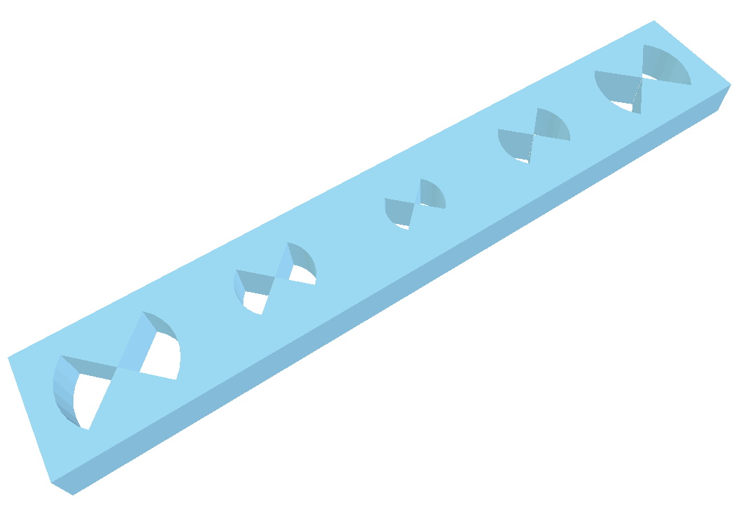
Physical Review Applied 15.3 (2021): 034029Solid state atom-like systems have great promise for linear optic quantum computing and quantum communication but are burdened by phonon sidebands and broadening due to surface charges. Nevertheless, coupling to a small mode volume cavity would allow high rates of extraction from even highly dephased emitters. We consider the nitrogen vacancy centre in diamond, a system understood to have a poor quantum optics interface with highly distinguishable photons, and design a silicon nitride cavity that allows 99 % efficient extraction of photons at 200 K with an indistinguishability of > 50%, improvable by external filtering. We analyse our design using FDTD simulations, and treat optical emission using a cavity QED master equation valid at and beyond strong coupling and which includes both ZPL broadening and sideband emission. The simulated design is compact (< 10 um), and owing to its planar geometry, can be fabricated using standard silicon processes. Our work therefore points towards scalable fabrication of non-cryogenic atom-like efficient sources of indistinguishable photons.
Arxiv link at https://arxiv.org/abs/2005.13478 -
Single photon emission and single spin coherence of a nitrogen vacancy center encapsulated in silicon nitride
Joe A Smith, Jorge Monroy-Ruz, John G Rarity, Krishna C Balram
Applied Physics Letters 116.13 (2020):134001Finding the right material platform for engineering efficient photonic interfaces to solid state emitters has been a long-standing bottleneck for scaling up solid state quantum systems. In this work, we demonstrate that nitrogen-rich silicon nitride, with its low background auto-fluorescence at visible wavelengths, is a viable quantum photonics platform by showing that nitrogen vacancy centres embedded in nanodiamonds preserve both their quantum optical and spin properties post-encapsulation. Given the variety of high-performance photonic components already demonstrated in silicon nitride, our work opens up a new avenue for building integrated photonic circuits using solid state emitters.
See the AIP Scilight companion piece
Arxiv link at https://arxiv.org/abs/1909.09383 -
Charge transfer properties through graphene for applications in gaseous detectors
S Franchino, D Gonzalez-Diaz, R Hall-Wilton, RB Jackman, H Muller, TT Nguyen, R de Oliveira, E Oliveri, D Pfeiffer, F Resnati, L Ropelewski, J Smith, M van Stenis, C Streli, P Thuiner, R Veenhof
Nuclear Instruments and Methods in Physics Research Section A: Accelerators, Spectrometers, Detectors and Associated Equipment 824 (2016): 571-574.Graphene is a single layer of carbon atoms arranged in a honeycomb lattice with remarkable mechanical and electrical properties. Regarded as the thinnest and narrowest conductive mesh, it has drastically different transmission behaviours when bombarded with electrons and ions in vacuum. This property, if confirmed in gas, may be a definitive solution for the ion back-flow problem in gaseous detectors. In order to ascertain this aspect, graphene layers of dimensions of about 2×2 cm2, grown on a copper substrate, are transferred onto a flat metal surface with holes, so that the graphene layer is freely suspended. The graphene and the support are installed into a gaseous detector equipped with a triple Gaseous Electron Multiplier (GEM), and the transparency properties to electrons and ions are studied in gas as a function of the electric fields. The techniques to produce the graphene samples are described, and we report on preliminary tests of graphene-coated GEMs.
Arxiv link at https://arxiv.org/abs/1503.06596 -
Efficient spin-photon interfaces for distributing entanglement
Joe A Smith
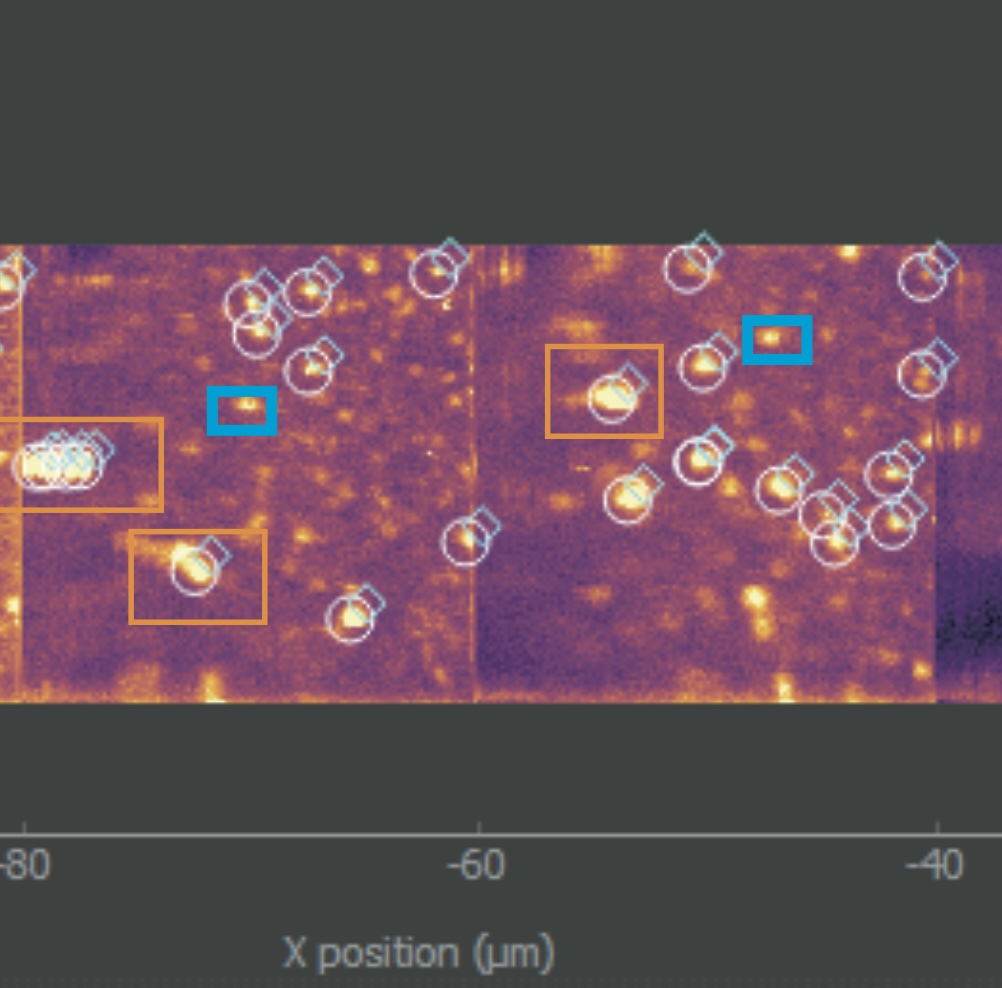
PhD thesis (2019)At last, use for quantum entanglement is on the horizon. Large computer companies race to build small quantum computers, usually based on superconducting circuits. The most elusive but rewarding of quantum-enabled technologies, however, would be the spin-photon interface for distributing entanglement. Elusive because single atoms are hard to isolate, and put into scalable systems. Rewarding because distributing entanglement over networks, using modular nodes, would result in quantum information resources that scale exponentially with the number of connected nodes. This in-built complexity would be unrivalled once proven. To do this, viable spin-photon interfaces will require harnessing established semiconductor technologies – integrating nanophotonics to filter and manipulate light and integrating nanoelectronics to provide the control of atom-like spins and classical processing of information. The Nitrogen Vacancy (NV) centre in diamond is perhaps the best understood optically-accessible atom-like system in a semiconductor and has been demonstrated as a spin-photon interface by entangling separate NV centres over a kilometre photonic channel. In this thesis, I borrow computational techniques to rapidly find and characterise NV centres with applications for large scale integration. For the first time, I evidence successful incorporation with a silicon-compatible platform, by encapsulating NV centres in nitrogen-rich silicon nitride by which the atom-like emitter would strongly couple to the centre of the silicon nitride waveguide mode. I measure the quantum signatures of single photon anti-bunching and electron spin Rabi oscillations of the same NV centre before and after deposition of 100 nm of PECVD nitride. Following this, I iterate to a mature out-coupler through planar lithography towards a scalable free space atom-photon interface in this platform. Finally, I consider how spin-photon interfaces could be improved, even above liquid-helium temperatures, and develop a novel planar cavity that will produce indistinguishable photons at Peltier-cooled temperatures, a further economic necessity for distributing entanglement over large networks.
