About me

About me

I am a researcher designing silicon chips to connect and control single spins currently based in QET Labs, University of Bristol, UK. My background is in engineering with a MEng in Electronic Engineering with Nanotechnology from UCL in 2014. Following a Kennedy scholarship year at MIT, I received my PhD in 2020 from the University of Bristol.

Our lab looks to create useful applications from physics experiments with the injection of technologies. One target is answering whether single atom-like defects in solids can be controlled at scale, by borrowing existing semiconductor processing tools. We use silicon photonics, microwave electronics and robotics as well as ambient and cryogenic confocal microscopes.

Recent work has looked at embedding atom-like systems in photonics, designing new photonic nanocavities and demonstrating compatibility with silicon photonics. I am also interested in engineering applied to spins, through scalable microwave control using multi-layer silicon electronics, and advancing quantum sensing by aligning large vector fields with robotics.

The research goal here is to put photonics and electronics front and centre: with useful applications in adding spins to photonic quantum computing and networks, but also for more near-term implications for high resolution quantum sensing. I am currently Researcher Co-Investigator and budget holder of a three year project called QC:SCALE - Quantum Circuits: Systematically Controlling And Linking Emitters for integrated solid state photonics platforms where we are developing technology to integrate atom-like systems with silicon electronics and photonics.


About me
About me
About me

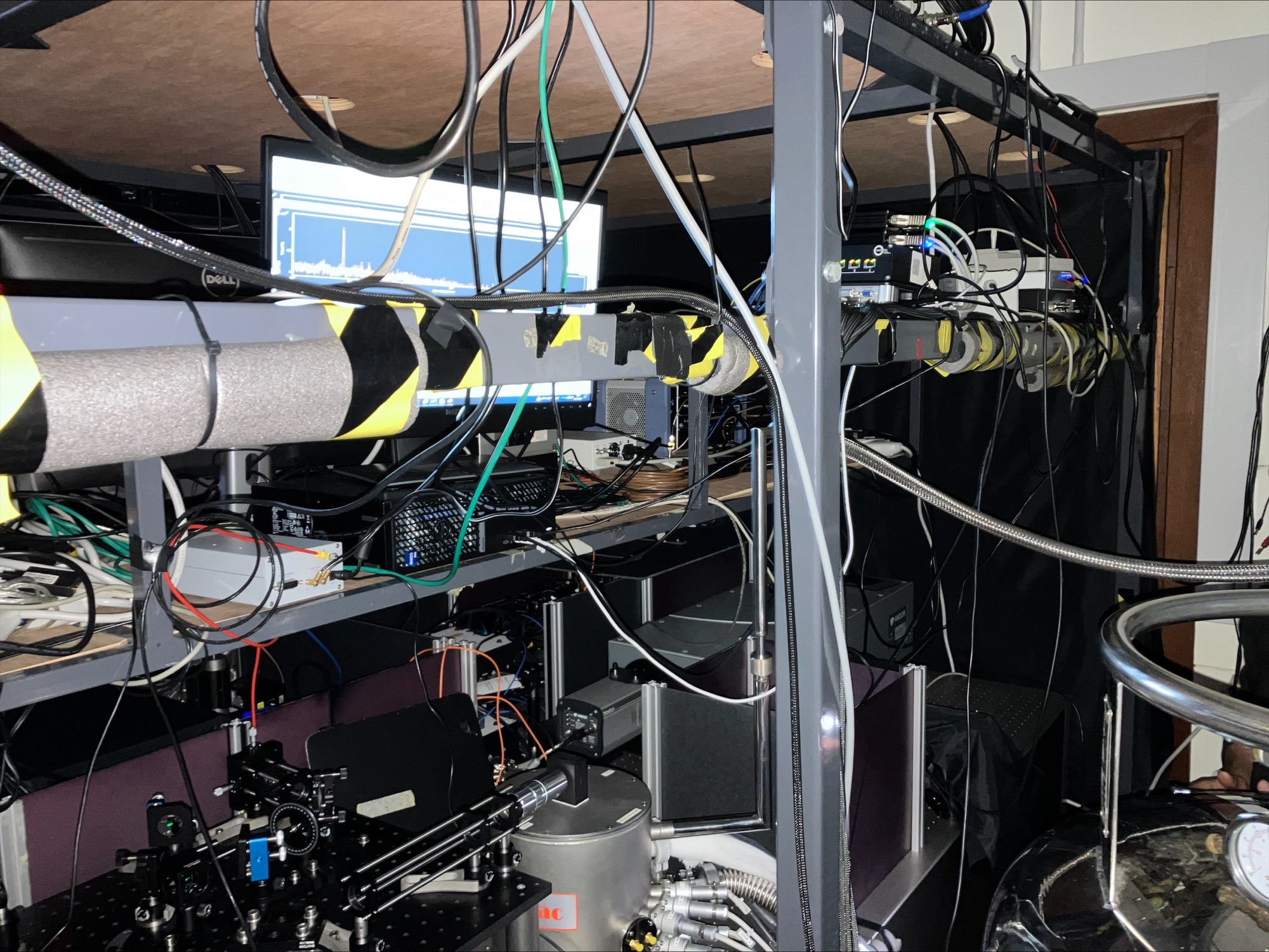
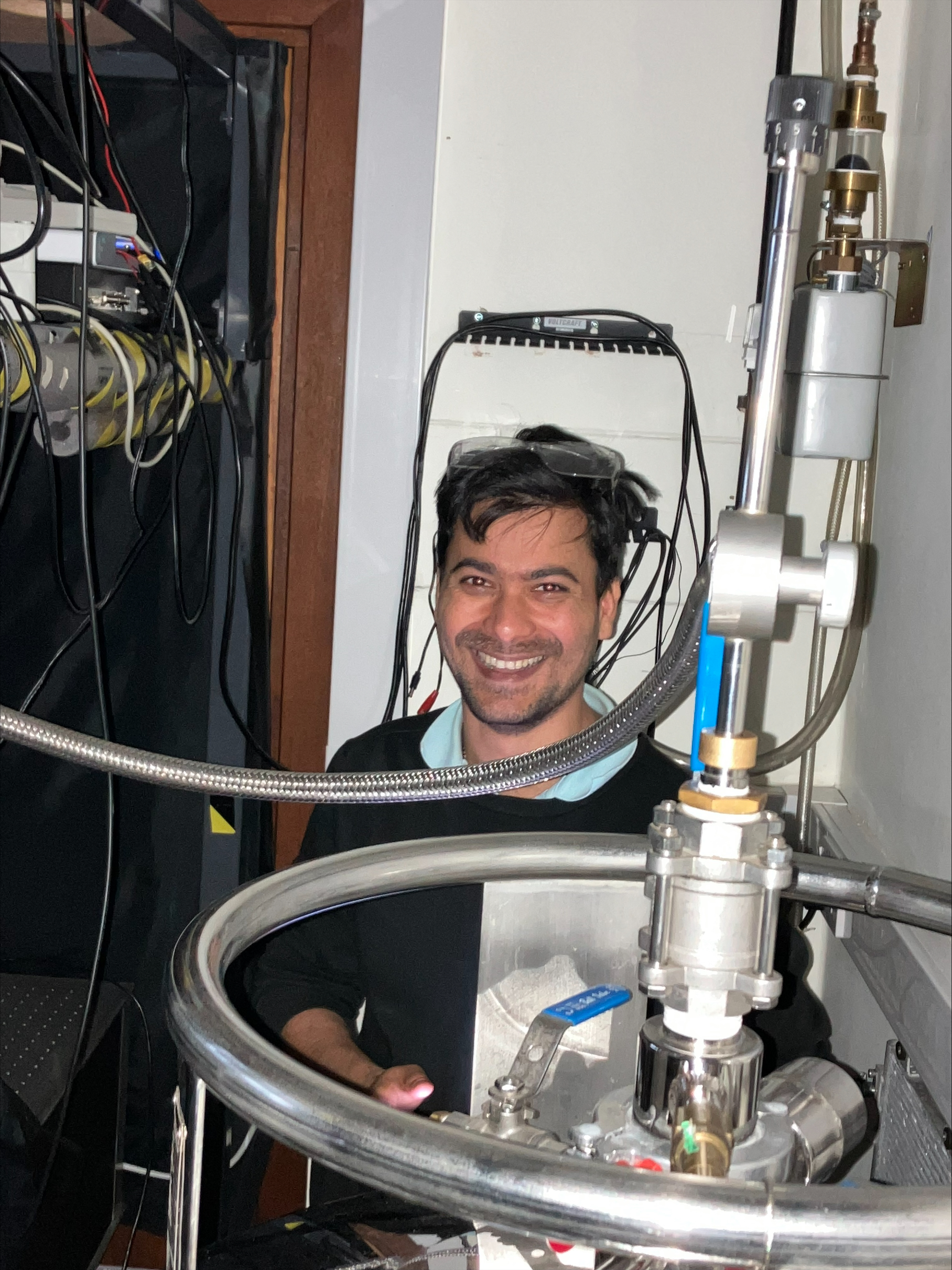
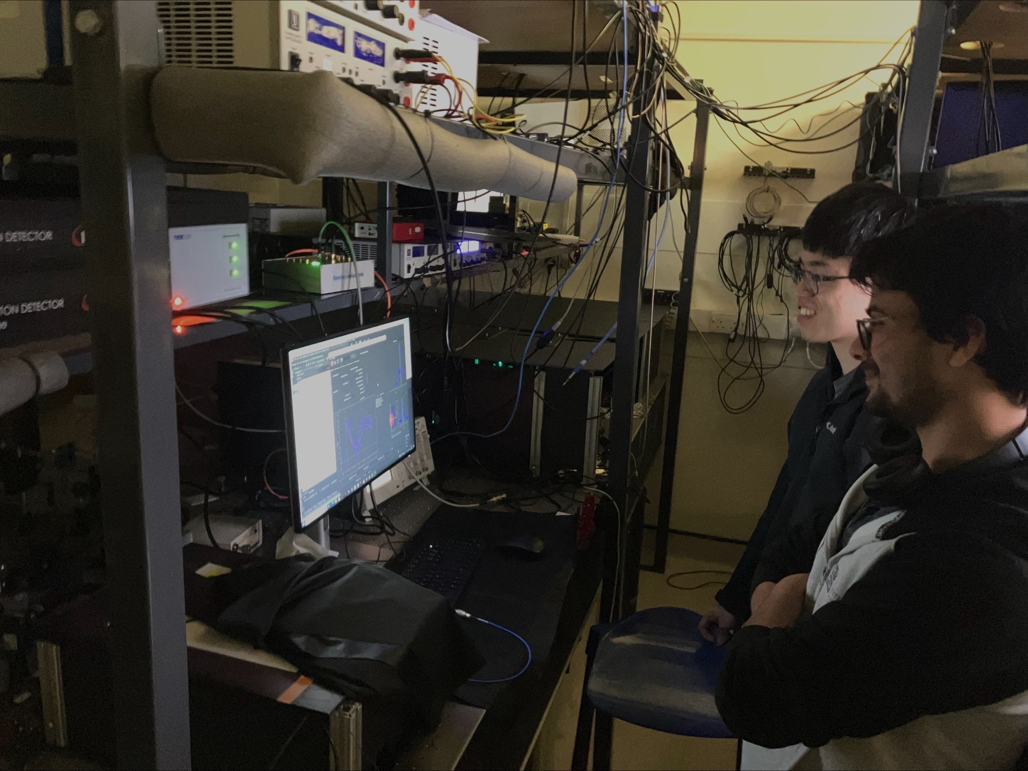
Pictures from the lab in 2023: Vivek Tiwari measuring an NV centre PL at 10 K; Hao-Cheng Weng performing a Rabi oscillation